OASIC-AQUA
Advanced Photonics Testbed at MIT
A DARPA OASIC testbed being established to bridge integrated photonics and neutral-atom quantum systems, with initial capabilities targeted for Fall 2026.

Scalable quantum computation requires tight integration between atomic physics and photonics engineering—two fields with historically distinct tools, and performance metrics. This laboratory seeks to integrate advanced photonic devices directly into a working atom-array testbed to co-evolve both technologies toward deployable quantum hardware.
Platform roadmap — estimated completion Fall 2026
- 1000 trapped rubidium atoms including atom motion control and readout.
- Closed-loop feedback between atom-array diagnostics and photonic device parameters for in-situ optimisation.
- Multiple wavelengths supported for simultaneous characterisation of devices for the D1, trapping, and Rydberg excitation bands.
- Electronic integration pathway with dedicated CMOS ASICs for low-latency control, signal processing, and feedback.
- We seek to establish stringent, quantitative performance metrics for standardised component certification.
We welcome early input from prospective collaborators on technical requirements and integration constraints that should shape these capabilities.
The platform is currently under development. We are seeking input from prospective collaborators to ensure the design meets the needs of the photonics and atomic physics communities. Below is the planned architecture—we welcome feedback on specifications, interfaces, and capabilities.
Planned integration modules
- Module A — 795 nm (D1 transition)
- Module B — 800–860 nm (optical trapping)
- Module C — >1 μm (Rydberg excitation pathways)
Each module provides free-space optical ports, a temperature-stabilised sample carrier, and ≥32 RF / ≥32 DC signal lines. The planned excitation pathway couples light into the device under test via holographically generated arbitrary intensity patterns, supporting vertically coupled light interfaces. Post-device beam-shaping is provided by a spatial light modulator capable of reshaping the output before imaging onto the atom array.
These baseline capabilities are designed to accommodate a broad range of photonic devices. The rendering below illustrates this optical configuration. If they do not exactly match your requirements, we welcome the opportunity to adapt the platform to your needs.
Virtual pre-integration with Optiverse
Optiverse is an interactive ray-tracing tool being developed alongside the platform. Collaborators can specify beam parameters, alignment tolerances, and mechanical constraints against the full optical model to validate compatibility of their chips, devices, and subsystems before integration.
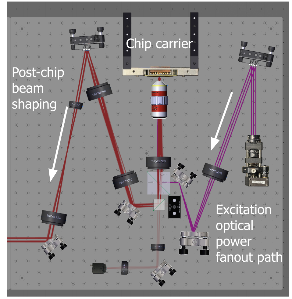
Optical excitation pathway: chip carrier, post-chip beam shaping, and excitation power fanout.
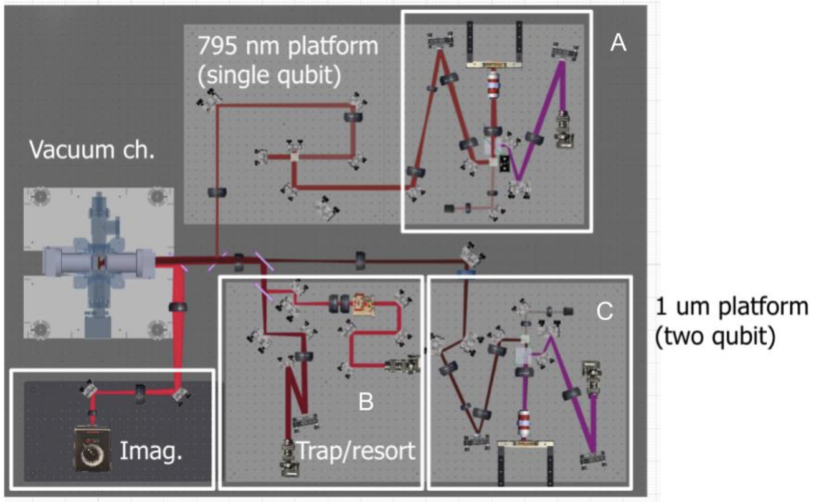
Full testbed layout (under design/construction): 795 nm and 1 μm platforms, vacuum chamber, trapping, re-sorting, and imaging subsystems.
Envisioned collaboration pathway
- Submit device specifications for virtual compatibility assessment via Optiverse.
- Ship devices and components to our MIT site for benchmarking against atom-array references.
- Run certification tests and receive standardised data.
Intellectual property protection
We understand that industry collaborators require robust safeguards for proprietary technology. All collaborative engagements are supported by the MIT Technology Licensing Office, which works with partners to establish appropriate agreements protecting company intellectual property throughout the integration and testing process.
We are actively seeking input on what collaborators need from this platform. Whether you have a specific device in mind or want to help shape the specifications, we would like to hear from you.